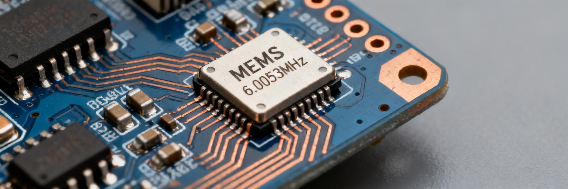
The DSA612RI1A-027HTVAO is a programmable clock device class with one or more LVCMOS outputs, a supply range centered on 1.8–3.3 V and minimum output frequency down to 0.001 MHz for low-power timing applications. Point: key numeric takeaways include supply 1.8–3.3 V, output types LVCMOS, typical ICC-active in the low mA range, and ppm-level stability. Evidence: these are the critical datapoints engineers extract from a datasheet. Explanation: they drive decisions on supply routing, decoupling and thermal margins.
Point: this introduction frames the primary verification targets for bench work: frequency accuracy, jitter and supply current. Evidence: the following sections map exactly which datasheet figures to capture and how to present them. Explanation: engineers benefit from a concise checklist before PCB spin to reduce rework and meet system timing budgets.
Product overview & essential electrical parameters

Package, pinout & signal names
Point: list packages (e.g., 8-pin UDFN, 6-pin SOT) and pin functions with explicit VCC, GND, outputs and control pins as called in the datasheet. Evidence: the datasheet identifies VCC (power), GND (return), OUTx (clock outputs) and EN/SEL (enable/select) pins and suggests footprint land pattern. Explanation: include recommended footprint callouts (pad size, solder mask, thermal pad) and mark VCC/GND and decoupling placement to ensure manufacturability and thermal path.
Supply voltage, operating temperature & DC limits
Point: present recommended supply range (1.8–3.3 V typical), absolute min/max (e.g., 1.7 V min, 3.6 V max), and operating temperature range (e.g., -40°C to +85°C). Evidence: datasheet sections for Absolute Maximum Ratings and Recommended Operating Conditions provide these numbers and typical vs. max notation. Explanation: report typical values with test conditions (VCC, TA) and separate worst-case (absolute max) margins; recommend at least 10% headroom from absolute max for robust designs.
Detailed clock output specifications
Frequency range, stability & pull range (PPM)
Point: specify output frequency range (min → max, e.g., 1 kHz → 200 MHz), whether outputs are fixed or programmable, and trimming/pull range in ppm (e.g., ±50 ppm). Evidence: the datasheet's Electrical Characteristics lists frequency limits, programmable register map and pull-range figure; clock specs such as initial tolerance and tempco are often tabulated. Explanation: present typical vs. worst-case stability by quoting nominal stability at 25°C and worst-case across full temp and VCC range, and describe method for measuring stability with a frequency counter over temperature sweep.
Output logic levels, rise/fall times, jitter & phase noise
Point: define logic family (LVCMOS), VOH/VOL at VCC=1.8 V and 3.3 V, rise/fall times (e.g., 0.5–2.0 ns), RMS jitter (ps) and phase noise reference offsets. Evidence: datasheet tables provide VOH/VOL at specified IO loads, rise/fall measured into 10 kΩ//15 pF, and jitter measured over 12 kHz–20 MHz integration. Explanation: include measurement conditions (load, termination, VCC, temperature) and advise extracting both RMS jitter and phase-noise curves or single-sideband phase-noise points for system margin calculations.
Power consumption & thermal behavior
Active, standby and control-mode currents
Point: extract ICC-active (mA), ICC-standby (µA–mA) and currents in low-power modes (µA). Evidence: datasheet current tables list test conditions (VCC, frequency, EN high/low). Explanation: report currents alongside conditions (e.g., VCC=3.3 V, fOUT=27 MHz, TA=25°C); provide a sample table layout for clarity:
| Mode | Test Conditions | Current |
|---|---|---|
| Active | VCC=3.3V, fOUT=27 MHz, IO=No load | ~6 mA (typ) |
| Standby | VCC=3.3V, EN=0 | ≤5 µA (typ) |
| Low-power | VCC=1.8V, fOUT=1 kHz | ~0.8 mA (typ) |
Power dissipation, thermal derating & decoupling recommendations
Point: calculate PD = VCC × ICC for representative cases and add worst-case margins. Evidence: using ICC-active 6 mA at 3.3 V, PD ≈ 19.8 mW; worst-case scenarios scale with higher IO loading. Explanation: provide PCB copper recommendations (e.g., 2–4 mm² thermal pad, stitched vias), recommend decoupling (0.1 µF ceramic + 1 µF tantalum close to VCC pin) and describe measurement setup to isolate device current (Kelvin sense resistor or high-side current meter).
Design & PCB implementation guidance for reliable clock performance
Power supply filtering, bypassing & layout do’s
Point: actionable layout rules: place a 0.1 µF X7R ceramic within 1–2 mm of VCC pin and a 1 µF bulk capacitor on the supply rail; stitch ground vias under the thermal pad. Evidence: datasheet recommends decoupling and shows layout examples; empirical practice reduces supply impedance and jitter. Explanation: instruct shortest return paths to the ground plane, use via stitching for thermal relief and place high-frequency bypass caps adjacent to VCC and GND pins to suppress supply transients.
Clock routing, impedance, termination & EMI mitigation
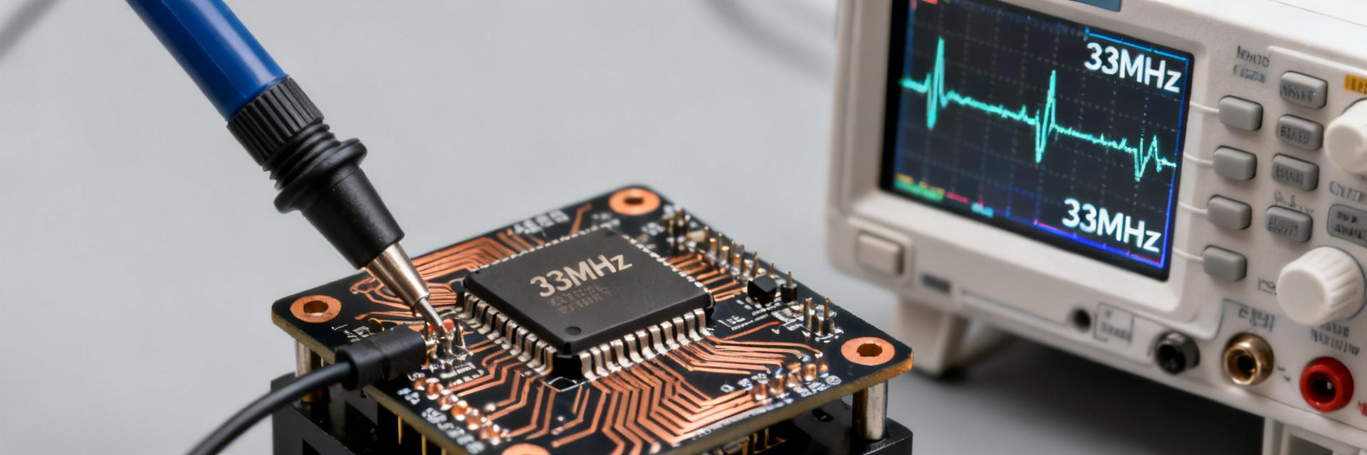
Point: route single-ended traces with 50 Ω characteristic impedance and apply series source termination (22–33 Ω) near the output for overshoot control; for differential outputs use 100 Ω differential. Evidence: datasheet output drive specs and recommended terminations give rise/fall and reflections guidance. Explanation: keep traces short, avoid parallel runs with noisy signals, use ground pours, and verify with oscilloscope and spectrum analyzer; scope probe tip-and-barrel methods are recommended to minimize loading when measuring jitter and edges.
Test cases, verification checklist & application notes
Recommended bench measurements and setups
Point: step-by-step tests: frequency accuracy with a frequency counter, RMS jitter with a phase-noise analyzer or jitter meter, and supply current with a source-measure unit (SMU). Evidence: datasheet provides pass/fail thresholds for each metric under specific conditions (VCC, TA). Explanation: include probe loading notes (use 10x passive probes or active probes with <2 pF), specify instruments (counter with <0.1 ppm accuracy) and acceptance criteria tied to datasheet worst-case values.
Pre-production checklist & common gotchas
Point: checklist items: footprint verification, pin mapping, supply sequencing, decoupling presence, thermal via stitching, and termination correctness. Evidence: common failures are mismatched termination and missing decoupling, which manifest as excess jitter or current draw. Explanation: validate each item on the checklist during first article build and run thermal and EMI scans to catch issues early.
Summary
- The DSA612RI1A-027HTVAO provides LVCMOS outputs with a recommended supply of 1.8–3.3 V and low-mA active current—verify ICC-active, standby current and PD from the datasheet figures.
- Key clock specs to confirm are frequency range, ppm stability and RMS jitter under specified load and temperature; measure both typical and worst-case values.
- PCB implementation priorities: local decoupling (0.1 µF + 1 µF), short return paths, thermal via stitching and proper terminations to control EMI and edge integrity.
- First checks for engineers: frequency stability, jitter and supply current—these three datasheet figures determine suitability for system timing and power budgets.
FAQ
What are the DSA612RI1A-027HTVAO power consumption expectations?
Typical active current is in the low single-digit milliamps at nominal VCC and mid-range frequencies; standby drops to microamps. Measure ICC with the device clocking at target frequency and with recommended decoupling, report VCC, TA and IO loading to match datasheet conditions for apples-to-apples comparison.
How to interpret DSA612RI1A-027HTVAO jitter specifications?
Jitter is provided as RMS over a specified integration band (e.g., 12 kHz–20 MHz) with test loads defined. To validate, use a jitter analyzer with the same integration range, identical termination and probe techniques; compare typical and worst-case numbers across temperature and supply variations.
What PCB layout tips ensure DSA612RI1A-027HTVAO clock performance?
Place a 0.1 µF ceramic capacitor within 1–2 mm of VCC to GND, use a local 1 µF bulk, stitch ground vias, route clock traces as controlled-impedance lines (50 Ω single-ended), and add source termination near the output. Verify with time-domain and spectrum measurements to confirm EMI and edge integrity.
How to resolve high-frequency reflections and clock overshoot in DSA612RI1A-027HTVAO designs?
To mitigate transmission line reflections and signal overshoot, place a 22 Ω to 33 Ω series termination resistor physically close to the LVCMOS output pin. Ensure the transmission line is designed as a 50 Ω single-ended trace and routed over a clean, continuous ground reference plane with no splits.