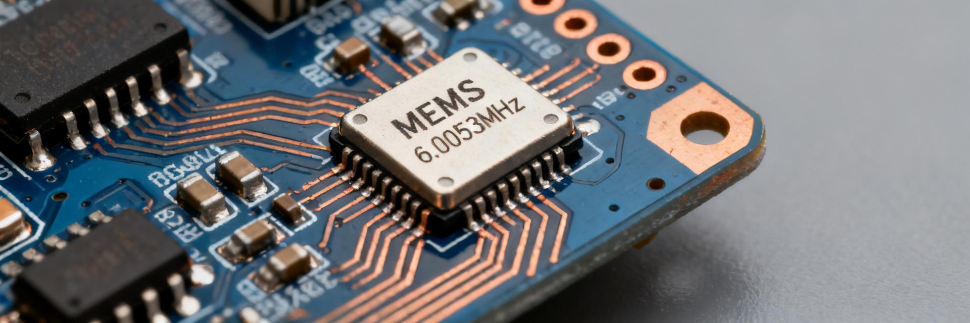
The DSA1001DI1-006.0053VAO is a 6.0053 MHz MEMS/LVCMOS timing device whose low-power and small-footprint specs make it a common choice where board area and battery life matter. This article summarizes the official datasheet and pinout, highlights the critical electrical performance numbers you need for integration, and gives a practical checklist for design and troubleshooting. The part string DSA1001DI1-006.0053VAO is shown here to anchor the discussion for engineers reviewing a datasheet or board layout.
Overview & Key Specifications (datasheet snapshot)
Part summary & ordering options
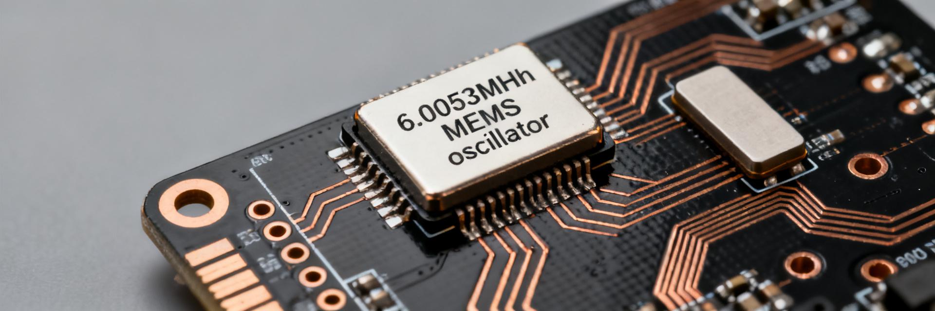
Point: The DSA1001DI1 family is a compact MEMS oscillator line; this 6.0053 MHz variant delivers a single-ended LVCMOS clock in a small package. Evidence: The datasheet lists the factory-programmed frequency, tolerance class, and package/thermal grade for board-level ordering. Explanation: For procurement and BOM control, ordering must match the exact frequency and tolerance/ppm class; this variant is a 6.0053 MHz device with factory-specified tolerance and low-power standby capability noted in the datasheet.
Electrical highlights (nominal values)
Point: Key nominal electrical values determine integration constraints. Evidence: The datasheet presents supply range, currents, output type, startup time, frequency tolerance and operating temperature. Explanation: Below is a compact table of those nominal figures you should confirm against the specific datasheet revision before prototype sign-off.
| Parameter | Nominal / Typical | Notes (datasheet) |
|---|---|---|
| Supply voltage | 1.7 V – 3.6 V | Verify min/max per datasheet for family variants |
| Supply current (active) | ~0.6 mA (typ, 3.3 V) | Measure at specified VCC and load |
| Standby current | <1 µA (typ) | When standby/power-down enabled |
| Output logic | LVCMOS single-ended | Drive strength and load conditions in datasheet |
| Startup time | ~2 ms typical (max ≤10 ms) | Time to stable oscillation after VCC or enable |
| Frequency tolerance | ±50 ppm (initial) | Factory tolerance class; see datasheet for options |
| Operating temperature | -40 °C to +85 °C | Commercial/industrial grade per datasheet |
Electrical Characteristics & Performance (detailed datasheet section)
Frequency behavior & stability
Point: Frequency vs. temperature, initial accuracy and aging drive clock reliability. Evidence: The datasheet specifies temperature coefficient curves, initial tolerance (ppm), aging (ppm/year) and jitter/phase-noise figures under defined conditions. Explanation: Expect initial tolerance in the ±10–100 ppm family window, aging on the order of ±1 ppm/year, and RMS jitter in the low picoseconds for a MEMS/LVCMOS oscillator; measure with a jitter analyzer using the datasheet's stated load (typically 15 pF), VCC and temperature to reproduce published numbers.
Recommended test method: use a high-resolution jitter analyzer or spectrum analyzer with time-interval error measurement, set input coupling to DC, measure over the datasheet-specified gate/load and temperature points, and compare typical vs. worst-case numbers. Typical vs. worst-case: datasheet gives both typical and maximum values—validate both during qualification.
Power, startup & reliability figures
Point: Active and standby power, sequencing, startup time and reliability metrics affect system power budgeting and production test. Evidence: The datasheet lists active/standby currents, startup time to valid output, and any supply-sequencing notes; some variants include MTBF or qualification references. Explanation: For battery-powered designs, budget for active current during operation and virtually negligible standby current when disabled; observe any recommended supply sequencing and note the specified startup window for host timing requirements.
Pinout & Mechanical Dimensions for DSA1001DI1-006.0053VAO
Pin functions & electrical connections (pinout)
Point: Correct pin connections and EP treatment are critical for device function and EMC. Evidence: The datasheet provides a pin map and recommended PCB tie-down for ground/EP. Explanation: Use the following table as a recommended pin mapping; confirm the datasheet for your package variant and apply the EP as the primary thermal/ground connection.
| Pin | Symbol | Function | Recommended connection |
|---|---|---|---|
| 1 | NC | No connect / reserved | Leave floating / follow datasheet |
| 2 | GND | Device ground | Direct via to PCB ground plane |
| 3 | OUT | LVCMOS clock output | Route to load with series resistor if required |
| 4 | EN | Enable / standby control | Pull high/low per datasheet; use MCU control or tie to VCC |
| 5 | VCC | Supply voltage | Bypass close to pin; follow decoupling guidance |
| EP | EXPOSED PAD | Thermal/ground | Solder to ground plane with vias |
Package drawing, land pattern & soldering notes
Point: Mechanical tolerances and soldering recommendations safeguard yield. Evidence: Datasheet includes package dimensions, recommended land pattern and reflow profile. Explanation: Follow footprint tolerances and stencil aperture recommendations; typical MEMS packages require a conservative paste coverage on the EP (60–80%) with 0.12 mm stencil thickness. Use thermal vias under the EP filled or capped and stitched to ground. For reflow, follow JEDEC-style ramp and peak temperature guidance from the datasheet and respect ESD handling procedures during assembly.
Integration & Typical Application Circuits
Clock distribution, decoupling & layout best practices
Point: Layout dictates jitter, EMI and signal integrity. Evidence: The datasheet calls out decoupling and load conditions; manufacturer notes recommend capacitor placement. Explanation: Place a 0.01–0.1 µF high-frequency ceramic decoupling capacitor within 1 mm of VCC to GND and optionally a 1 µF bulk capacitor on the rail. Route the output trace with controlled impedance, minimize stub length and avoid routing under noisy power nets. A small series resistor (22–33 Ω) at OUT can damp reflections when driving multiple loads.
Example schematics: MCU clock, low-power systems
Point: Two common application scenarios are a direct MCU clock and a low-power system using enable/standby. Evidence: The datasheet defines EN/standby behavior and output drive. Explanation: (1) MCU clock: tie EN to VCC, route OUT through 22 Ω to MCU clock pin, decouple VCC with 0.01 µF near the device. (2) Low-power: tie EN to a GPIO to assert standby; when EN is deasserted, device enters µA standby per datasheet—ensure MCU waits the datasheet startup time before sampling the clock.
Design Checklist, Compliance & Troubleshooting
Pre-production validation checklist
Point: A concise lab checklist shortens debug cycles. Evidence: Datasheet numbers provide pass/fail thresholds for frequency, jitter, current and thermal behavior. Explanation: Validate frequency and jitter vs. datasheet limits, measure active/standby current, run supply margin tests (VCC min/max), perform thermal cycling across the operating range, and verify land pattern and solder joints with X-ray or optical inspection. Define pass/fail criteria tied to datasheet max/min specifications.
Common issues & fixes
Point: Typical integration faults are addressable with targeted diagnostics. Evidence: Datasheet and pinout notes reveal causes such as incorrect EP grounding or missing decoupling. Explanation: No output — check VCC, EN state and solder joints on EP; unstable frequency or excessive jitter — verify decoupling placement, output loading and routing stubs; wrong voltage levels — confirm supply range and VCC sequencing. Use the datasheet and pinout to map pin functions while troubleshooting.
Summary
The DSA1001DI1-006.0053VAO delivers a compact, low-power 6.0053 MHz timing solution—this outline has summarized the essential datasheet specs, pinout, integration guidance, and a practical validation checklist so engineers can move quickly from datasheet to prototype. When preparing a prototype, verify the supply range, active/standby current, startup time and EP grounding against the datasheet and check the pinout mapping carefully during layout.