Designers selecting board-level clocks need concise datasheet validation: roughly half of modern serializer/ADC front ends and RF IF chains require low-jitter, board-mounted oscillators to meet link budgets and demodulator phase-noise budgets. This deep-dive targets hardware engineers, PCB designers, and validation engineers integrating the DSA1123DA1 318.75MHz LVDS oscillator, covering key specs, timing, layout, test methods, and selection checklist.
1 — Background & product overview (background introduction)
The DSA1123DA1 is a fixed-frequency, LVDS-output oscillator commonly specified at 318.75MHz; designers should confirm the LVDS oscillator interface and 6-VDFN footprint early. This section extracts the sheet’s identifiers and clarifies ordering-code reading, helping teams map part variants to system clock trees and supply domains.
Key datasheet identifiers & nominal specs
| Parameter | Nominal / Typical |
|---|---|
| Nominal frequency | 318.75 MHz |
| Output type | LVDS differential |
| Supply voltage | VCC = 3.3 V (typical) |
| Enable/Disable | Logic-controlled enable pin (active state per ordering) |
| Package | 6-pin VDFN (exposed pad) |
| Operating temp | Commercial/extended ranges (check ordering) |
| Typical power | ~80–120 mW (active); low-standby current |
Reading ordering codes: identify frequency suffix, temperature grade, and packaging code. Verify variant suffixes for enable polarity or tightened jitter bins. Treat listed typical currents as baseline; budget worst-case maximums shown in electrical tables for thermal design.
When to choose this oscillator (system-level fit)
Choose this unit when a fixed, low-jitter 318.75MHz clock with LVDS output fits serializer or IF boards, digital radios, or ADC sampling schemes. It pairs with LVDS receivers or differential clock inputs and is suitable where a compact 6-VDFN footprint and controlled start-up behavior are required in hierarchical clock trees.
2 — Electrical & timing characteristics (data analysis)
LVDS output behaviour and interface details
Datasheet LVDS outputs typically specify differential amplitude (around 350–600 mVpp), common-mode window (≈1.1–1.6 V), and source/sink drive. Designers should plan AC or DC coupling consistent with receiver common-mode tolerance; a matched differential termination (100 Ω across the pair) at receiver pins minimizes reflections and preserves amplitude margins.
Supply, enable/disable and power budgets
VCC tolerance often allows ±5% around 3.3 V; confirm absolute max. Enable pin logic levels determine active-high/low behavior and any internal pull direction. Use the datasheet’s typical and standby current figures to compute steady-state and worst-case power; include start-up current and specified start-up time when sequencing multi-domain supplies and thermal budgets.
3 — Frequency stability, phase noise & jitter analysis (data analysis)
Frequency stability specs—initial tolerance, temperature drift (ppm/°C), and aging—define timing margins for synchronous systems using the 318.75MHz clock. Translate ppm figures into absolute timing error and phase shift across operating range to size PLL capture windows and SERDES tracking loops.
Frequency tolerance, temperature coefficient and aging
Interpret ppm specs as fractional error: 1 ppm at 318.75MHz equals ~318.75 Hz. Temperature curves and stated aging (ppm/year) map into required PLL bandwidth or retiming tolerances. Engineers convert these into phase margin budgets and hold-off periods for systems that rely on tight absolute frequency over temperature.
Phase noise and RMS jitter: system impact
Phase-noise plots (SSB dBc/Hz vs offset) should be integrated across the system bandwidth to yield RMS jitter. For example, integrated phase noise from 12 kHz–20 MHz producing 0.5 ps RMS can be compared against ADC aperture jitter or SERDES eye closure budgets; allocate jitter margin between source, board, and PLL elements.
4 — PCB integration & layout best practices (method guide)
Footprint, grounding and decoupling
Follow the datasheet land-pattern for the 6-VDFN; ensure exposed pad is soldered with via stitching to ground. Place a 0.1 µF ceramic decoupling capacitor within 0.5 mm of VCC, add a 1 µF bulk nearby, and use multiple vias on the pad for thermal relief. Maintain a solid ground plane beneath to minimize return-path impedance.
LVDS routing and termination strategy
Route LVDS as a controlled-impedance differential pair (target 100 Ω differential), minimize skew by matching pair lengths to within a few mils for clock inputs, place differential termination at the receiver, and locate AC-coupling capacitors only if the receiver requires them. Avoid crossing noisy power traces beneath the pair.
5 — Testing, validation & troubleshooting (method guide / case)
Bench tests to verify datasheet performance
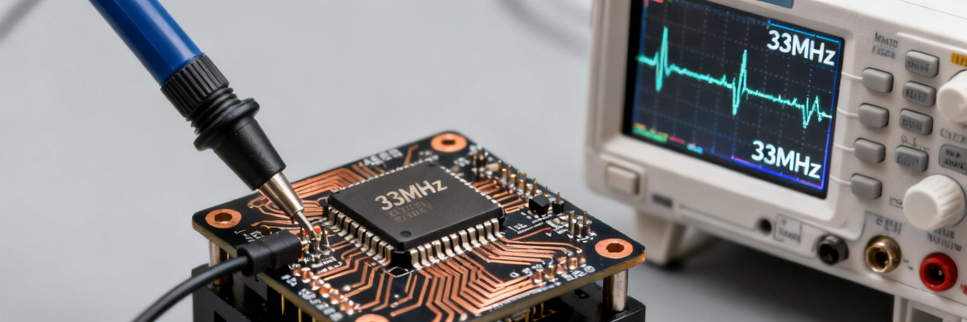
Key equipment: frequency counter, spectrum analyzer with phase-noise option, time-interval analyzer for RMS jitter, and low-noise power supply. Measure frequency, phase noise (SSB), integrated jitter over specified bands, supply sensitivity, enable behavior, and start-up time. Record environmental stress runs for thermal stability validation.
Common integration issues and fixes
Typical problems include no output (check enable polarity and supply sequencing), excessive jitter (verify termination, supply noise, and ground returns), amplitude swings (ensure correct common-mode range and termination), and intermittent start-up (inspect solder joints and reflow profile). Use methodical isolation to root-cause board-induced EMI.
6 — Application examples & selection checklist (case + action)
Representative application scenarios
- High-speed ADC front end clocking: key spec is low RMS jitter to preserve SNR and SFDR during conversion and sampling.
- IF-stage local oscillator for downconversion: phase noise near carrier offsets determines demodulator BER and close-in spurs.
- Clock distribution to LVDS receivers in serializer networks: output amplitude and termination compatibility ensure clean eye diagrams.
Quick selection and procurement checklist
- Verify nominal frequency: 318.75MHz matches system plan and PLL/serdes expectations.
- Confirm interface: LVDS oscillator output and receiver common-mode/termination compatibility.
- Check jitter & phase-noise specs against ADC/SERDES budgets and required integration band.
- Validate package: 6-VDFN land-pattern and thermal pad alignment for PCB footprint.
- Confirm VCC, enable polarity, operating temperature grade, and request test reports before final assembly.
Summary
- Verify the DSA1123DA1 nominal frequency, LVDS oscillator interface, and package footprint early; mismatch in any of these increases redesign risk and impacts clock distribution.
- Use phase-noise plots and ppm stability figures to derive integrated RMS jitter and thermal frequency drift margins for PLLs and ADC front ends.
- Follow 6-VDFN layout, decoupling, and differential routing best practices; validate with spectrum and time-interval measurements during prototype testing.
Frequently Asked Questions
What are the key verification steps for DSA1123DA1 jitter and phase noise?
Measure SSB phase noise on a spectrum analyzer with an appropriate phase-noise option, integrate across your system bandwidth to compute RMS jitter, and cross-check with a time-interval analyzer. Perform supply sensitivity and enable sequencing tests to confirm worst-case jitter under real operating conditions.
How should PCB designers handle the 6-VDFN footprint for the 318.75MHz LVDS oscillator?
Adopt the datasheet land-pattern exactly, solder the exposed pad with thermal vias to ground, place decoupling within 0.5 mm of VCC, and maintain a continuous ground plane beneath. Ensure differential pair exits are impedance-controlled and length-matched to receiver inputs.
What supply and enable considerations affect startup for the LVDS oscillator?
Check VCC tolerance and absolute maximum ratings, respect enable pin polarity and any internal pull direction, and follow recommended supply sequencing. Measure start-up time to stable output and include that in system boot timelines and PLL-lock sequencing to avoid metastability.
What termination scheme is recommended for the 318.75MHz LVDS clock signal?
A standard 100-ohm differential termination resistor must be placed as close as possible to the receiver input pins. This matches the differential trace impedance and suppresses reflections, preserving the signal integrity of the 318.75MHz clock.