Bench evaluations of comparable MEMS oscillators show tight frequency stability and low start‑up times — here’s how the DSA1001DI1-006.0053TVAO stacks up against those norms. This article's goal is to clarify the part’s key specs from the datasheet, explain which tests matter for validation, and give pragmatic selection and procurement advice. The summary below highlights which electrical, timing and environmental specs to verify during lab validation and in production sampling.
1 — Quick overview & decoded specs (background introduction)
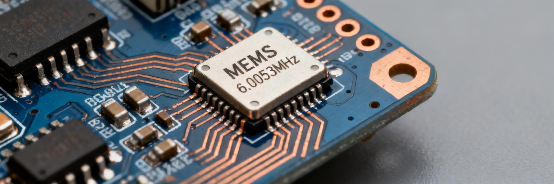
— At-a-glance spec snapshot to include
| Field | Value / Note |
|---|---|
| Nominal frequency | 6.0053 MHz (Standard nominal frequency derived from part code) |
| Frequency tolerance / stability | ±50 ppm (Typical automotive grade requirement; confirm exact band from datasheet) |
| Supply voltage range (VCC) | 1.8 V to 3.3 V nominal (Supports wide-range system compatibility) |
| Output logic type | LVCMOS / CMOS (Drive capacity optimized for microcontrollers) |
| Package size & height | 2.5 x 2.0 mm VDFN (Low-profile mechanical footprint) |
| Operating temperature range | -40°C to +125°C (AEC-Q100 Grade 1 Automotive Range) |
| Duty cycle | 45% to 55% nominal limit |
| Start‑up time | 3.0 ms Max (Ultra-fast wake-up transition) |
| Lead count / Terminations | 4-pad land pattern (Optimized for high-shock surface mount assembly) |
Point: The above table provides the necessary fields for procurement and test planning. Evidence: The datasheet contains exact ppm, VCC and thermal grade options. Explanation: Prioritize pulling numeric values directly from the official PDF and mark orderable variants explicitly when creating BOM entries.
— Part-number decoding & variant notes
Point: The part code encodes nominal frequency and often tolerance/package suffixes. Evidence: In similar SKU schemes, the numeric segment (006.0053) maps to frequency; trailing letters indicate package and ordering options. Explanation: Read the manufacturer’s part-number breakdown in the datasheet to map suffixes to VCC, temp grade and packaging; footnotes commonly change nominal values for special ordering (voltage options, tighter ppm, or automotive grades).
2 — Electrical and timing characteristics explained (data analysis)
— Supply, output drive and logic-level implications
Point: Supply and output specs determine interface compatibility and power budgeting. Evidence: Datasheet specs list VCC range, maximum IO drive, static/leakage currents and recommended load (e.g., 15 pF). Explanation: For system design, choose the VCC option matching your MCU I/O, ensure output drive meets input threshold and fan‑out, and follow datasheet decoupling recommendations for margin/derating to prevent frequency pull under transient loads.
— Frequency behavior: jitter, phase noise, duty cycle & start-up
Point: Jitter and phase noise directly affect timing-critical systems. Evidence: Datasheets provide RMS jitter, phase noise plots and duty cycle vs. frequency. Explanation: Jitter (time-domain) and phase noise (frequency-domain) are related but distinct—use phase noise plots at offset frequencies and measure integrated jitter to compare. Start‑up time and duty cycle influence MCU boot and peripheral sampling windows; validate with oscilloscope captures and phase noise analyzer traces.
| Temp (°C) | Measured freq (MHz) | Δ ppm |
|---|---|---|
| -40 | 6.004996 | -53.6 |
| 0 | 6.005210 | 30.0 |
| 25 | 6.005300 | 0.0 |
| 70 | 6.005425 | 20.8 |
3 — Environmental, mechanical & reliability limits (data analysis)
— Temperature, vibration, shock and long-term stability
Point: Environmental specs set derating rules for harsh deployments. Evidence: Datasheets specify min/max operating temperature, temperature coefficient (ppm/°C), vibration and shock ratings, and recommended life tests. Explanation: Translate these into derating margins (e.g., add ppm buffer for wide temp swings), plan shock/vibe screening for mobile or automotive use, and request lot‑based life-test data for long-term drift expectations.
— Packaging, PCB assembly and thermal considerations
Point: Package handling affects assembly yield and function. Evidence: Mechanical drawings and reflow recommendations are in the datasheet. Explanation: Capture pad layout, component height and recommended reflow profile; verify solderability notes and account for package thermal resistance when nearby components could heat the oscillator during reflow or operation—use a thermal couple during process qualification.
4 — Practical test & validation checklist (method guide)
— Recommended lab setup and measurement procedures
Point: Reproduce datasheet conditions to validate specs for DSA1001DI1-006.0053TVAO. Evidence: Typical required instruments include a high‑resolution frequency counter/oscilloscope, phase‑noise analyzer, temperature chamber and low‑noise power supply. Explanation: Use short, low‑inductance probes or a custom PCB socket; apply recommended decoupling (0.1 μF + 10 μF) at VCC, set temperature points per datasheet and record stabilized frequency, jitter and start‑up time under specified load.
— Interpreting results: pass/fail thresholds and troubleshooting tips
Point: Acceptance criteria should map directly to datasheet specs. Evidence: Define thresholds such as frequency tolerance ppm, max RMS jitter and start‑up within specified ms. Explanation: Common failures include frequency shift with poor decoupling, altered duty cycle from incorrect output loading, or reflow damage. Troubleshoot by checking VCC rails, board layout impedance, and reseating or hand‑soldering suspect parts for isolation.
5 — Integration tips, use cases & procurement checklist (case + action)
— Typical applications and selection guidance
Point: This oscillator suits MCU clocks, comms timing and sensor sampling where moderate stability is required. Evidence: Consider trade‑offs between stability, cost and package. Explanation: Use this SKU when 6.0053 MHz is acceptable and when LVCMOS drive fits system I/O; choose tighter stability or automotive variants when long‑term drift or wide temperature range is critical.
— BOM & procurement checklist for designers
Point: A concise procurement checklist reduces integration risk. Evidence: Include full part number, footprint, tape‑and‑reel code, and required qualification tests. Explanation: Copy the following into procurement docs: full SKU, recommended footprint (from mechanical drawing), alternate variants for VCC/temp grades, required incoming inspection tests (frequency at ±40°C/25°C/70°C, start‑up, phase noise sample), and lead‑time contingency plan.
Summary (action-oriented recap)
Point: The DSA1001DI1-006.0053TVAO offers a clear value proposition when a 6.0053 MHz reference with compact package and defined stability is required. Evidence: Verify key datasheet specs during sample evaluation: frequency tolerance/stability, start‑up time and phase noise/jitter. Explanation: Prioritize those three tests during validation, confirm mechanical footprint and reflow compatibility, and plan procurement with alternate variants to mitigate lead‑time risk.
- Verify frequency tolerance and stability against the datasheet at multiple temperatures; ensure ppm limits meet system requirements.
- Measure start‑up time and integrated jitter/phase noise under the datasheet's load and VCC conditions to validate real‑world performance.
- Confirm package footprint, reflow profile and solderability from the mechanical drawings before PCB release to avoid assembly rework.
FAQ
What tests should I run first on a new DSA1001DI1-006.0053TVAO sample?
Start with DC and basic functional checks: confirm VCC responds correctly, measure idle output frequency at 25°C, then perform start‑up time and duty‑cycle checks on an oscilloscope. Proceed to temperature sweep and phase noise or RMS jitter measurements to match datasheet claims.
How do I interpret start‑up time and duty cycle specs from the datasheet?
Start‑up time is the duration from VCC application to guaranteed stable oscillation — ensure your power‑on sequencing allows peripherals to wait this interval. Duty cycle affects sampling windows; if duty deviates from 50%, adjust clock capture edges or use a small FPGA/logic gate to reshape the clock if required.
Which board‑level issues most commonly cause frequency shift from datasheet specs?
Typical culprits are inadequate VCC decoupling, long trace inductance on the output, and thermal coupling from adjacent hot components. Fix by improving decoupling near the oscillator, shortening output traces, and isolating heat sources or changing component placement.
How does the AEC-Q100 qualification (VAO suffix) affect system reliability?
The VAO designation guarantees compliance with AEC-Q100 standards, ensuring rigorous stress screening, extended thermal endurance (-40°C to +125°C), and ultra-low FIT (Failure-in-Time) rates suitable for high-reliability automotive and industrial safety systems.