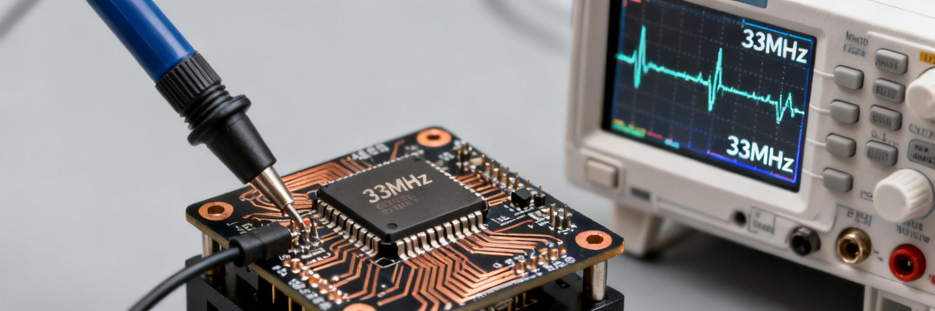
Adding a stable 156.25 MHz clock to a high-speed design introduces common pain points: unwanted jitter, level mismatches, and PCB-induced noise. This guide presents a practical, stepwise integration plan for the DSA1224BL2 part, focusing on electrical checks, PCB layout, power/enable sequencing, and validation. It emphasizes measurable checkpoints engineers can apply immediately to reduce integration risk when introducing a MEMS oscillator into Ethernet, SERDES, or FPGA clock trees.
Experience-driven recommendations below draw on lab best practices and field troubleshooting patterns. Where values vary by variant, the guide flags what to confirm in the vendor datasheet and what to treat as conservative starting points for prototyping and test. Engineers will find a short table of key electrical items, a simple block schematic, PCB layout notes, and a compact integration checklist for build sign-off.
1 — Why choose the DSA1224BL2 for 156.25 MHz designs (background)
Key use cases and advantages
Fixed 156.25 MHz clocks are common for Ethernet PHY reference clocks, SERDES reference sources, and some telecom or FPGA domain clocks. Choosing this oscillator type simplifies timing for PHYs and SERDES PLL inputs and removes the fragility of discrete crystal oscillators. Compared with crystals, a MEMS oscillator offers better mechanical resilience, shorter lead times, and built-in frequency trimming options; designers should still verify frequency tolerance and jitter requirements against system budgets before selection.
Required pre-checks before selecting the part
Before committing to the part, confirm package pinout and land-pattern compatibility, required IO standard (HCSL, CMOS, LVDS, etc.), nominal supply voltage, and enable-pin behavior. Also verify available frequency tolerance and jitter class options. For procurement and BOM stability, include a "156.25 MHz MEMS oscillator selection checklist" in the part-approval step to capture these electrical and mechanical constraints.
2 — Electrical specifications & timing characteristics (data)
Essential electrical parameters to validate
Key electrical items are nominal VCC (commonly 3.3V), typical and maximum supply current, logic IO thresholds for enable and output, and absolute maximum ratings. Place local decoupling close to the VCC pad—typically a 0.1 µF ceramic in parallel with a 4.7–10 µF bulk capacitor within a few millimeters of the device. Always confirm absolute-max and thermal derating in the datasheet before finalizing the supply routing and plane strategy.
Timing specs that impact integration
Validate output format (single-ended CMOS/HCSL or differential LVDS/LVPECL), rise/fall times, RMS phase jitter, period stability, and start-up time. Match the jitter budget of the receiving PLL or SERDES: low-picosecond RMS jitter is typically required for high-speed SERDES; ensure the oscillator's spec fits the overall link budget. Use the part's start-up time to sequence enable signals and avoid false locks in downstream PLLs.
3 — Signal integrity and interface considerations (data)
Matching the oscillator output to your clock receiver
Termination depends on output type: CMOS often needs a pull-up/pull-down or series damping; HCSL and LVPECL require specific AC/DC terminations; LVDS needs 100 Ω differential across the receiver. For single-ended outputs, add a small series resistor (20–33 Ω) at the source for damping. Avoid heavy fanout; if the clock must feed several devices, use a low-jitter clock buffer or distributor to preserve amplitude and edge integrity.
PCB trace handling for high-speed clock lines
Treat the clock trace as a controlled-impedance route: 50 Ω single-ended or 100 Ω differential as required. Keep lengths short and matched for differential pairs, minimize stubs, and avoid crossing splits in ground/power planes. Stitch ground vias near transitions and use via-in-pad sparingly. Validate traces with a TDR and capture an eye or jitter measurement at the receiver to verify signal integrity before large-volume release.
4 — PCB integration: footprint, layout and placement (method)
Footprint and mechanical placement
Place the oscillator as close as practical to the primary clock consumer to reduce trace length and exposure to switching noise. Orient the device so differential/single-ended pins route directly to the receiver with minimal vias. Respect the manufacturer's recommended land pattern and mechanical keepouts and consider thermal relief if the device will be near hot components or airflow constraints.
Power decoupling and ground strategy
Use a 0.1 µF ceramic decoupler and a 4.7–10 µF bulk capacitor per oscillator supply, placed within 2–5 mm of the VCC pad. Prefer a solid local plane for return; avoid routing high-current switching traces under the oscillator. Add ground stitching vias around the device to isolate it from noisy domains and reduce loop area for clock traces.
5 — Power sequencing, enable behavior and EMI mitigation (method)
Power-up / power-down and enable pin handling
Sequence power so VCC reaches nominal before asserting enable. Use a defined pull-up or pull-down on the enable pin (10 kΩ is a common starting value) to ensure the oscillator remains disabled during brown-out or reset conditions. Account for start-up time in system firmware: do not deassert downstream resets until the oscillator output is stable and within expected frequency and jitter bounds.
EMI and filtering best practices
Small RC filters (e.g., 10–100 Ω series with 10–100 pF to ground) on enable or auxiliary pins can reduce conducted emissions, but avoid over-filtering that delays enable edges or increases start-up time. For radiated emissions, keep clock traces short, use ground pours with via stitching, and measure conducted/radiated emissions with and without the oscillator to isolate its contribution.
6 — Validation, troubleshooting and integration checklist (action / case)
Essential bench tests and acceptance criteria
Key bench tests: verify frequency accuracy at operating temperature, measure RMS jitter with a jitter analyzer, check rise/fall times and duty cycle on a high-bandwidth scope, and confirm enable/disable timing. Establish pass/fail thresholds aligned with system jitter budget and receiver lock requirements. Use proper probes and termination during measurement to avoid adding measurement artifacts.
Common integration issues and fixes
Typical problems include excessive jitter caused by noisy supplies (fix with improved decoupling and low-ESR caps), missing clock due to incorrect enable sequencing or wrong output type (verify pin logic and IO standard), and reflections from improper termination (add source damping or correct termination network). Final sign-off checklist should include footprint verification, decoupling, termination, power sequencing validation, jitter within budget, and EMI test plan.
Block schematic (concept):
VCC --[0.1µF + 4.7µF]--> DSA1224BL2 VCC
EN --[10k pull-up]--> DSA1224BL2 EN
OUT --[22Ω series]--> clock receiver (with proper termination)
| Item | Typical/Guideline |
|---|---|
| Supply | 3.3 V nominal (confirm datasheet) |
| Supply current | Tentative < 30 mA; confirm variant |
| Output types | CMOS / HCSL / differential options |
| Duty cycle | ~50% ±5% |
| Decoupling | 0.1 µF + 4.7–10 µF within 2–5 mm |
Summary
- Verify electrical specs and IO format early to match receiver requirements and avoid rework when integrating the DSA1224BL2 part into a clock tree.
- Manage signal integrity with controlled-impedance traces, minimal stubs, and appropriate termination; add a buffer if fanout exceeds safe limits.
- Place decoupling close to VCC, use conservative enable pull resistors, and sequence power so the clock is stable before releasing downstream resets.
- Validate with frequency, jitter, and EMI tests; use an integration checklist to capture footprint, decoupling, termination, sequencing, and test thresholds before production.
Frequently Asked Questions
What are recommended PCB decoupling practices for a MEMS oscillator?
Place a 0.1 µF ceramic decoupler in parallel with a 4.7–10 µF bulk capacitor within a few millimeters of the VCC pad, route return directly to a solid ground plane, and avoid routing noisy switching supplies under the device. These steps reduce supply-induced jitter and improve start-up stability.
How should the enable pin be handled for reliable start-up of a MEMS oscillator?
Use a defined pull resistor (10 kΩ is a typical starting point) so the device is held in a known state during power transitions. Ensure VCC reaches its nominal value before asserting enable, and allow the oscillator's specified start-up time before deasserting downstream resets to avoid false locks.
What measurements should be run to validate oscillator integration?
Measure frequency accuracy, RMS jitter with a jitter analyzer, rise/fall times on a high-bandwidth scope, and verify enable/disable behavior. For SI checks, run TDR on clock traces and capture an eye diagram or phase noise as required by the receiver's jitter budget.
How do I minimize EMI and switching noise on the 156.25MHz clock lines?
Keep clock traces as short as possible, route them as controlled-impedance lines over a continuous ground plane, and avoid crossing plane splits. Implement small series damping resistors (20–33 Ω) at the source to control edge rates and minimize reflections.