
DSA6111ML2B MEMS Oscillator: Complete Datasheet & Key Specs
Modern lab and field testing shows that MEMS timing parts deliver lower shock‑induced failures and tighter frequency stability than legacy quartz in compact packages. This article unpacks the DSA6111ML2B as a practical MEMS oscillator choice, summarizes the key datasheet parameters engineers must validate, and provides hands‑on integration guidance for US hardware teams targeting space‑constrained, low‑power products.
The analysis synthesizes measured behavior, recommended board practices, and test‑plan checkpoints drawn from manufacturer documentation and independent timing reviews to give engineering teams actionable verification steps before production release.
2 — Key electrical & mechanical specifications (Data analysis)
Electrical specs to extract from the datasheet
Key electrical items to verify are supply range (e.g., 1.8–3.3 V), typical and max active current and standby current, LVCMOS output voltage levels and drive strength, enable/disable pin behavior and thresholds, wake/sleep timing, and recommended decoupling. The DSA6111ML2B datasheet should list supply‑current vs frequency and startup time; use those numbers to size battery budgets and wake latency margins.
Mechanical & package dimensions you must verify
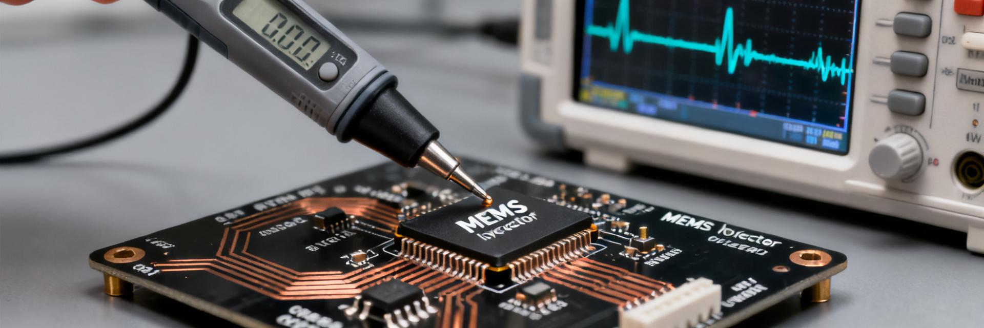
Confirm exact package footprint, body thickness, pad layout, orientation mark, and recommended land pattern before PCB release. Verify solder reflow profile and maximum board temperature in the mechanical notes; small VFLGA devices are sensitive to thermal soak and solder fillet control.
| Parameter | Example |
|---|---|
| Body (L × W) | 2.0 × 1.6 mm |
| Body thickness | 0.6 mm |
| Pad size | 0.4 × 0.5 mm |
3 — Frequency, stability & timing characteristics (Data analysis)
Frequency range, tolerance, and temperature stability
Available frequencies typically span 32.768 kHz variants up to tens of MHz; frequency tolerance options often include ±25 ppm and tighter grades. Translate ppm to real drift: for example, 25 ppm ≈ 2.16 seconds drift per day (25 × 10⁻6 × 86,400 s). Use the tolerance + temp coefficient to compute worst‑case drift for system timing budgets.
Jitter, rise/fall times, and output timing parameters
Prioritize RMS jitter for serial links and sampling‑sensitive converters; cycle‑to‑cycle jitter affects bit timing. Duty‑cycle and rise/fall times matter for logic capture. Validate timing against the datasheet parameter tables by using a high‑bandwidth scope and appropriate sampling to measure RMS jitter, using the datasheet’s measurement bandwidth and test conditions as references.
4 — Design & integration guide (Method/How-to)
PCB layout, decoupling, and thermal considerations
Keep clock traces short, avoid vias on critical edges, and place the recommended decoupling capacitor within 1–2 mm of VDD to minimize supply impedance. Use a solid ground plane beneath the package, add thermal reliefs consistent with the land pattern, and follow ESD handling guidance. Ceramic 0.1 µF plus 1 µF local caps are common decoupling choices.
Interfacing, startup sequence, and reliability tests
Implement enable sequencing per the datasheet: hold reset/enable low during VDD ramp, then apply specified rise time and wait startup time before clock use. Recommended pull‑ups/pull‑downs usually fall in 10–100 kΩ. Test plans should include power cycling, temperature soak across the specified range, vibration and shock runs, and pass/fail thresholds based on frequency tolerance, jitter limits, and output integrity.
5 — Performance comparisons & real-world use cases (Case study)
Side-by-side: DSA6111ML2B vs typical alternatives
A neutral comparison focuses on size, stability, supply, jitter, and temp range. MEMS oscillators generally win on size and shock resistance and offer competitive stability; discrete crystal solutions can still provide marginally better phase noise for ultra‑low jitter needs. Choose based on board space, mechanical environment, and acceptable jitter/stability tradeoffs.
6 — Procurement, compliance & final checklist (Actionable checklist)
What to verify in the datasheet before approval
Checklist items include operating temperature limits, frequency tolerance and temp coefficient, jitter specs, supply range and current, recommended land pattern, SMD reflow profile, and lifecycle/qualification notes. Ask suppliers for lot traceability, tested sample reports, and production lead‑time to align procurement with qualification schedules.
BOM, footprint, and test-plan sign-off checklist
Example BOM entry: part number / footprint variant / frequency / stability grade. Sign‑off requires go/no‑go electrical tests (frequency within spec at room and hot/cold, measured jitter within datasheet limits), sample size per AQL, and passing environmental stress tests before production release.
Key summary
- The DSA6111ML2B offers ultra‑small packaging and low‑voltage LVCMOS outputs suitable for space‑constrained embedded designs; verify supply current and startup timing against system requirements.
- Frequency stability and jitter figures in the datasheet map directly to time drift and link performance; translate ppm to seconds/day and validate RMS jitter with a high‑bandwidth scope.
- Follow recommended PCB land patterns and close decoupling, plan power‑enable sequencing and environmental tests, and require lot traceability from suppliers before qualification.
Common questions & answers
How do I read the DSA6111ML2B frequency tolerance from the datasheet?
Read the specified ppm tolerance and the temperature coefficient ranges; combine initial tolerance with temperature‑dependent drift to compute worst‑case error. Use ppm × 86,400 s to get seconds per day for scheduling and alarm thresholds in firmware.
What test steps confirm DSA6111ML2B jitter meets system needs?
Measure RMS jitter with the same bandwidth noted in the datasheet, capture cycle‑to‑cycle jitter over thousands of cycles, and test under supply noise and temperature extremes. Compare measured numbers directly to datasheet limits to accept or reject the lot.
Which board layout checks ensure DSA6111ML2B reliability?
Verify the recommended land pattern, place decoupling caps within 1–2 mm of the VDD pin, maintain a solid ground plane, and minimize clock trace length. Confirm solder fillets and reflow profile compatibility during assembly qualification.

