
MPF100TS-1FCVG484T2 Datasheet: Key Specs & Limits
The MPF100TS-1FCVG484T2 presents headline numbers that matter: roughly 109K logic elements, ~7.6 Mbit of embedded memory, a 484-ball BGA footprint and an industrial temperature grade—figures that directly drive package, power and thermal decisions for designers. This concise walkthrough highlights the critical specs and hard limits in the official datasheet so engineers can prioritize procurement checks, power sequencing, timing margin and thermal planning for robust mid‑density FPGA designs.
1 — Device overview & part ID (Background)
What this part is and where it fits
Point: The MPF100TS-1FCVG484T2 is a mid‑range FPGA class targeted at mid‑density datapath, control and edge compute roles.
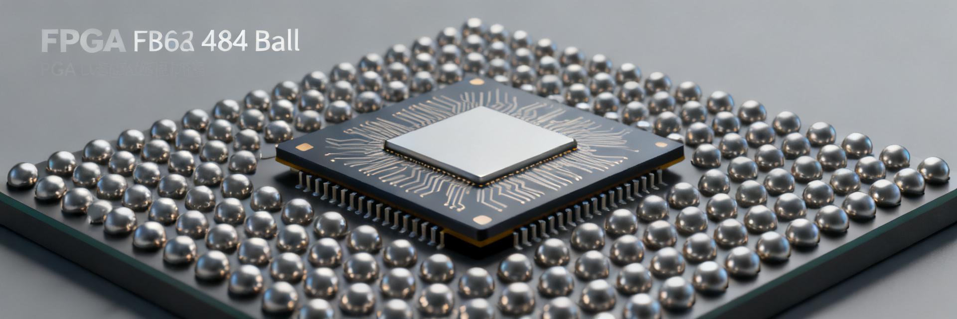
Evidence: datasheet headline metrics list logic element count (~109K), embedded RAM (~7.6 Mbit), and a 484‑ball BGA package.
Explanation: those metrics imply a balance of capacity versus cost—enough LUT/register resources and RAM for moderate DSP and packet processing while remaining constrained by BGA routing density and BOM economics when compared to higher‑end devices.
Ordering/marking and variant notes
Point: The part suffix encodes temperature grade and package code and must be confirmed before procurement.
Evidence: the datasheet shows T/S or I grade suffixes and the FCVG484 package code used in ordering tables.
Explanation: verify datasheet ordering codes against vendor order tables; mismatched suffixes change guaranteed operating temperature and mechanical footprint, so confirm the exact ordering code in procurement to avoid costly rework.
2 — Electrical DC specs & absolute maximums (Data analysis)
DC supply rails & voltages
Point: Proper supply rails and sequencing are mandatory for reliable operation.
Evidence: the datasheet lists core rails near 1.0–1.05 V and multiple I/O bank rails with nominal voltages per bank.
Explanation: follow recommended nominal voltages and decoupling and respect sequencing notes to avoid latch‑up or configuration failure.
Absolute maximum ratings
Point: Absolute maximums define irreversible damage limits.
Evidence: consult the datasheet Absolute Maximum Ratings table for pin voltages, storage temperature and maximum VCC values.
Explanation: exceeding those limits risks permanent device damage; observe VIH/VIL and clamp diode behavior to stay within specified thresholds.
3 — Logic, memory and timing limits (Data analysis)
Logic fabric & embedded resources
Point: Resource accounting drives feasibility of a design fit. Evidence: the datasheet enumerates logic element count, LUT/register composition, ~7.6 Mbit embedded RAM, numbers of DSP blocks and PLLs in the resources table. Explanation: translate synthesis reports to these device resources early; routing congestion often limits final fit—plan for buffer/regrowth and reserve routing headroom.
Timing, max frequencies and clock architecture
Point: Clocking limits and jitter determine achievable throughput. Evidence: the datasheet provides recommended input clock rates, PLL performance and maximum IO/clock domain switching frequencies in timing tables. Explanation: design for worst‑case timing margin—apply negative slack margins, include jitter budgets and follow datasheet tables for PLL lock ranges.
4 — I/O, transceivers and interface limits (Method/guide)
I/O banks & Standards
Point: I/O bank organization constrains signal standards and mixing. Evidence: the datasheet specs list per‑bank voltage ranges for LVCMOS/LVTTL. Explanation: avoid unsupported mixed standards in a single bank and place decoupling close to each bank.
High-speed transceivers & SERDES
Point: SERDES lanes impose SI and clocking constraints. Evidence: the datasheet summarizes transceiver lane counts and supported line rates. Explanation: adhere to recommended reference clock quality and follow the datasheet’s eye‑mask and receiver limits.
5 — Packaging, thermal limits and design checklist (Actionable)
Mechanical, pinout and mounting constraints
Point: The 484‑ball BGA package drives PCB footprint and assembly rules. Evidence: the datasheet mechanical section gives nominal dimensions, ball pitch and soldering profile notes. Explanation: use the exact mechanical drawing for footprint generation and account for warpage/standoff limits.
Thermal management & practical design limits checklist
Point: Thermal strategy is essential for reliable margins. Evidence: the datasheet provides operating junction/ambient ranges and thermal resistance guidance. Explanation: implement thermal vias under the device, provide copper pours, and validate with margin testing.
Summary
- The MPF100TS-1FCVG484T2 headline limits—~109K logic elements, ~7.6 Mbit RAM and a 484‑ball BGA—drive routing, power and thermal tradeoffs.
- Key hard limits: absolute maximum ratings for pin voltages, required core and I/O rail nominal voltages, and thermal junction/ambient bounds.
- Design checklist: confirm ordering code, follow power sequencing, place decoupling per bank, and run worst‑case timing simulations.
FAQs
What core and I/O voltages does the MPF100TS-1FCVG484T2 require?
Answer: The device requires a core rail near 1.0–1.05 V and multiple I/O bank rails with nominal voltages outlined in the datasheet DC characteristics. Always copy the exact rail voltages and tolerances into your power‑supply BOM.
Where are the absolute maximum ratings found for MPF100TS-1FCVG484T2?
Answer: Absolute maximums are listed in the datasheet’s Absolute Maximum Ratings table—these include maximum pin voltages, storage temperatures and VCC limits. Treat those values as non‑negotiable.
What are the primary thermal limits to observe for MPF100TS-1FCVG484T2?
Answer: The datasheet’s thermal section lists operating junction/ambient temperature ranges and thermal resistance figures; use those numbers for power budgeting. Implement copper heat spread and thermal vias.

