
SiC MOSFET 3300V Thermal Optimization: Step-by-Step Guide
High junction temperatures, unexpected derating, and reliability loss in ultra-high-voltage converters are common pain points; this guide delivers a practical, step-by-step SiC MOSFET 3300V thermal optimization workflow to reduce Tj, increase MTBF, and avoid thermal runaway.
Evidence: Application notes and modeling studies emphasize structured characterization and thermal budgeting.
Explanation: Follow the steps below to convert measurements into robust cooling and protection decisions.
Point: Successful thermal optimization starts with targeted characterization and iterative design.
Evidence: Engineering literature and vendor design recommendations show measurement-driven improvements yield predictable junction margins.
Explanation: Designers should treat thermal optimization as an electrical design loop—measure losses, convert to ΔT with Zth, improve losses or cooling, then revalidate under worst-case pulses.
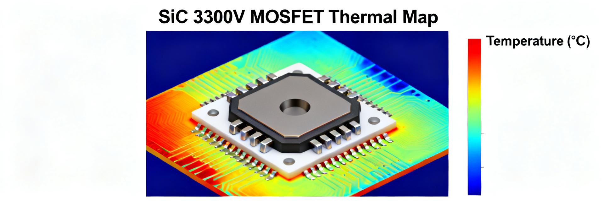
Background: Why thermal management matters for ultra-high-voltage SiC
Key thermal failure modes
Point: junction overheating drives the dominant failure modes. Evidence: documented issues include bond-wire lift, solder fatigue, thermal cycling damage, and short-circuit thermal runaway reported in module studies. Explanation: track metrics such as Tj_max, Tj_oper, power cycling count, and thermal resistance to assess MTBF and system-level derating reliably for 3300V SiC MOSFET reliability.
Thermal vs. electrical trade-offs
Point: 3300V devices have distinct trade-offs between die size, VDS stress, and switching-loss profiles. Evidence: high VDS requires larger die area and results in higher capacitances and switching overlap at high dv/dt. Explanation: gate-drive tuning, dv/dt control, and layout minimization of stray inductance directly reduce switching losses and thus thermal budget during transients.
Thermal Characterization & Limits
Essential Metrics
- ⚡ RθJA / RθJC (Thermal Resistance)
- ⏱️ Zth(j‑c)(t) (Transient Impedance)
- 🌡️ Tj_max (Junction Threshold)
How to quantify: Convert device power losses into ΔT and Tj using Zth. Evidence: standard calculation templates compute P_loss = P_cond + P_sw, then ΔT(t)=P_loss·Zth(j‑c)(t). reserve margin for worst-case transients and repetitive short-circuit energy limits.
Step-by-step thermal optimization workflow
Step 1: Minimize Generated Heat
Point: reduce switching and conduction losses first. Evidence: gate-drive optimization, rise/fall balance, deadtime tuning, snubbers, and low-inductance layout are effective loss reducers. Explanation: estimate switching losses from measured dv/dt and di/dt waveforms, iterate gate drive settings to trade EMI versus thermal gain.
Step 2: Improve Heat Evacuation
Point: choose cooling based on power density and system constraints. Evidence: forced air, board heat-sinks, heat pipes, and liquid cold plates rank by size, cost, and reliability. Explanation: use thermal vias under die attach, maximize copper area, and prefer solder/sinter interfaces or properly specified TIM with controlled assembly torque.
Practical Design Examples
Forced-Air Power Module
Point: numeric sizing turns targets into board features. Evidence: compute required RθJA from P_loss and allowable ΔT for Ta=40°F; fan CFM correlates to effective RθJA. Explanation: calculate heatsink area and via count to meet computed Tj targets.
Liquid-Cooled Cold Plate
Point: liquid cooling reduces RθJA for high-power density. Evidence: cold plate sizing uses coolant ΔT and flow assumptions. Explanation: account for pump selection and leak mitigation; validate thermal resistance chain from die to coolant.
Validation & Operational Checklist
Reliability Qualification
Point: a focused test matrix proves robustness. Evidence: tests include steady-state soak, transient pulse, power cycling, and thermal shock. Explanation: define pass/fail thresholds, instrument Tj probe locations, and log results to feed back into design.
On-board Protections
Point: integrate sensing and firmware derating. Evidence: temperature sensors near die attach and short-circuit detection timing. Explanation: monitor junction margin and implement automated derating curves in firmware to extend MTBF.
Summary & Key Takeaways
Following this workflow reduces Tj, improves reliability, and enables robust deployment of 3300V SiC devices. Recommendation: apply the steps now and revalidate MSC400SMA330D or equivalent devices.
- Measure First: Compute P_loss and convert to ΔT using Zth(j‑c)(t).
- Optimize Gate Drive: Balance rise/fall and minimize stray inductance.
- Match Cooling: Prioritize solder/sinter and thermal vias to lower contact resistance.

