The W25Q128JVEIQTR presents 128M‑bit serial NOR flash in a small SPI package with a 2.7–3.6 V supply window and a maximum standard SPI clock of 104 MHz. These headline numbers matter because they set capacity, voltage compatibility, and the baseline throughput engineers use for boot, XIP, or data‑log budgeting.
This article extracts the practical, engineer‑facing points from the datasheet—power envelopes, memory geometry, timing, package choices, PCB layout checks, and firmware integration steps—to speed schematic decisions, footprint selection, and firmware partitioning for embedded systems.
1 — W25Q128JVEIQTR at a glance: product snapshot (Background)
1.1 — One-line summary and intended applications
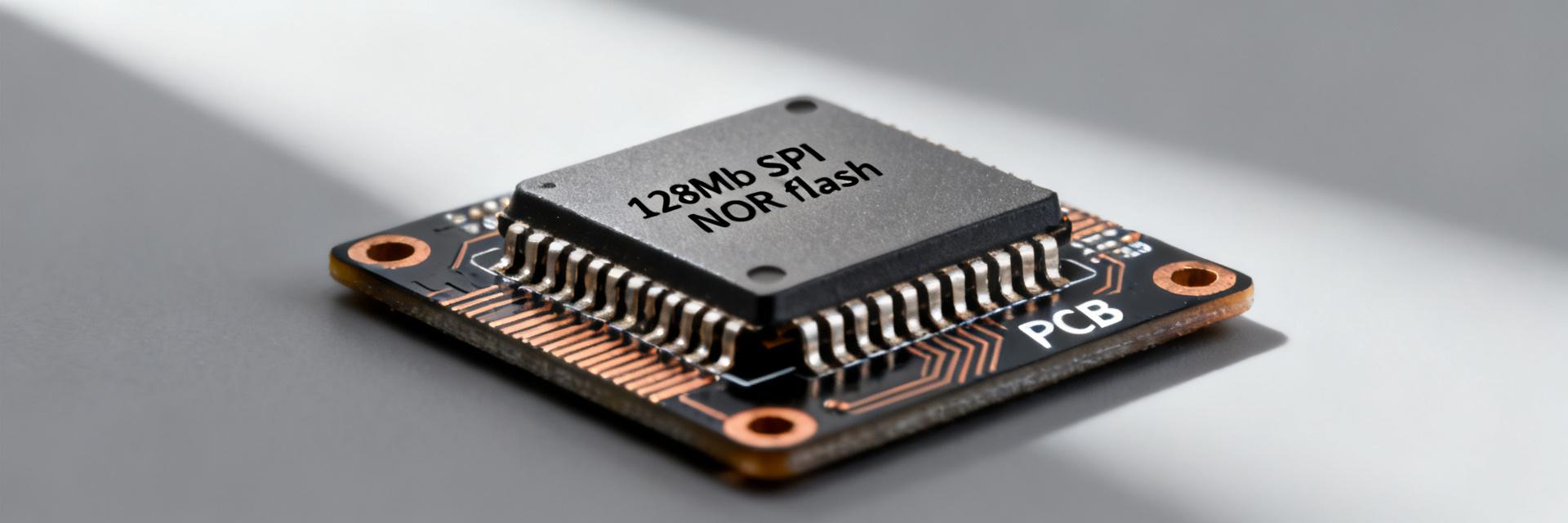
Point: A compact 128M‑bit serial NOR flash targeted at code and data storage. Evidence: 128M‑bit (16M x 8) organization and single‑supply 2.7–3.6 V compatibility. Explanation: Suited for MCU boot media, firmware storage, and data logging in low‑power sensors and consumer devices in the MCU classes that support SPI flash boot or XIP.
1.2 — Quick specs table to include in article (what to list)
Point: A one‑glance spec block speeds BOM and design decisions. Evidence: Core items below are those engineers expect to review first. Explanation: Drop this table into a BOM template or datasheet comparison spreadsheet for quick verification.
| Spec | Typical Value |
|---|---|
| Capacity | 128M‑bit (16M x 8) |
| Organization | 256‑byte page; 4KB sector; 32KB/64KB blocks |
| VCC | 2.7–3.6 V |
| Max clock | 104 MHz (standard SPI) |
| Interface | Single/Dual/Quad I/O, QPI modes |
| Package options | SOIC, WSON (select footprints) |
| Typical standby/active | Low µA standby; single‑digit mA active (datasheet ranges) |
2 — Key electrical and memory specifications from the datasheet (Data analysis)
2.1 — Power, voltage, and current: operating and standby figures
Point: Voltage range and current draw dictate power‑budget and decoupling. Evidence: Rated VCC 2.7–3.6 V; datasheet lists µA‑class standby and mA‑class active currents. Explanation: Plan decoupling at VCC with a 0.1 µF plus a 4.7 µF near the device, budget peak current for read bursts, and include margin for worst‑case active currents during flash programming.
2.2 — Memory organization, erase/program granularity, and endurance (128M‑bit specifics)
Point: Geometry and endurance drive wear‑leveling and update strategy. Evidence: 16M x 8 organization with 256‑byte page, 4KB sectors, and larger blocks. Explanation: Use sector‑level erase planning for data logs, reserve block regions for bootloader and fail‑safe images, and assume typical endurance cycles for NOR when designing update/rollback schemes and wear leveling.
3 — Performance modes, command set highlights & timing (Data analysis)
3.1 — Read/program/erase throughput and clock modes
Point: Interface mode selection determines practical throughput. Evidence: Standard SPI up to 104 MHz; dual/quad I/O and QPI increase bytes per clock. Explanation: For firmware budgeting, assume single‑I/O at nominal clock for conservative throughput; plan faster flash streaming or XIP with quad modes but validate signal integrity and MCU quad‑SPI controller support.
3.2 — Important timing and reliability parameters to capture from the datasheet
Point: Timing specs define signal margins and programming windows. Evidence: Critical parameters include tCS, tCH, tCL, tR, tPROG, and tERASE with program/erase times in ms range. Explanation: Record these values for driver timeouts, allow margin (×1.5 safety), and align PCB trace lengths and rise/fall targets to avoid timing violations at top clock rates.
4 — Pinout, package variants and PCB footprint guidance (Method/implementation)
4.1 — Common package options and how to choose one
Point: Package affects board area, thermal, and assembly. Evidence: Commonly available in SOIC and WSON packages with differing pad geometries. Explanation: Use SOIC for early prototyping and easy hand‑rework; choose WSON or smaller packages for production to save board area but ensure stencil/reflow and inspection processes are validated.
4.2 — Layout and routing checklist for reliable SPI operation
Point: Layout determines signal integrity at 104 MHz and above. Evidence: Recommended decoupling, short MOSI/MISO/SCLK lines, and proper WP/HOLD pull resistors are common datasheet guidance. Explanation: Place 0.1 µF cap within 1–2 mm of VCC pin, route SCLK with matched impedance and minimal stub lengths, stitch ground under the footprint, and add series resistors (22–33 Ω) on high‑speed lines if ringing appears.
5 — Integration checklist & typical firmware considerations (Method / Case study)
5.1 — Boot/bootloader and mapping best practices for 128M‑bit flash
Point: Logical mapping and partition strategy protect boot and enable updates. Evidence: 128M‑bit capacity supports multiple firmware images and data partitions. Explanation: Reserve a protected bootloader region, use a dual‑bank OTA layout with version and CRC metadata, and consider XIP only if the MCU supports execute‑in‑place and the board routing meets timing and noise constraints.
5.2 — Error handling, protection and secure update notes
Point: Datasheet protection bits and erase behaviors inform secure update flows. Evidence: Block protection features and status registers allow software write‑protect. Explanation: Implement CRC checks for images, use status‑register polling with timeouts for program/erase, mark protected regions, and design an update rollback path if validation fails after OTA flashing.
6 — Quick selection guide & practical recommendations for engineers (Actionable advice)
6.1 — How to verify a candidate on the bench (test plan)
Point: A short validation plan ensures part meets system needs. Evidence: Simple JEDEC ID read, read/write/erase timing checks, power‑cycle retention tests are effective. Explanation: Start with ID/JEDEC check, verify page program and sector erase times against expected worst‑case, perform repeated power cycling and retention checks, and monitor for error rates during stress.
6.2 — When to choose this part vs. alternatives (selection criteria)
Point: Clear decision bullets help part selection. Evidence: Choose 128M‑bit devices when capacity, quad‑SPI throughput, and 2.7–3.6 V support are required. Explanation: Prefer this part for mid‑range code and data storage with quad‑I/O needs; select different densities or NOR/NAND types when you need higher endurance, lower cost per bit, or raw page programming models.
Summary
The essential takeaways: 128M‑bit capacity in a 16M x 8 organization, single‑supply 2.7–3.6 V operation, and a standard SPI ceiling of 104 MHz define the core system constraints engineers must budget. Power envelopes, page/sector granularity, and timing parameters drive decoupling, firmware partitioning, and timeout values. Use the PCB checklist and the bench validation steps to confirm real‑world behavior before finalizing a BOM and layout. Copy the quick‑spec table into your BOM template and run the validation test plan on a prototype board to catch integration issues early.
Key Summary
- Capacity: 128M‑bit (16M x 8) — plan partitions for bootloader, application, and logs; consider wear‑leveling for frequent writes to sectors.
- Electrical: 2.7–3.6 V supply and µA standby vs. mA active — place decoupling near VCC and budget peak currents during program cycles.
- Performance: 104 MHz SPI baseline; use quad/Dual modes for higher effective throughput but validate signal integrity and MCU controller support.
Frequently Asked Questions
What key datasheet values should be logged for firmware using W25Q128JVEIQTR?
Log VCC min/max, active and standby current ranges, page/sector/block sizes, tPROG and tERASE typical/maximum, and command timing parameters (tCS, tCH, tCL, tR). Capture status‑register behaviors and block protection bits to implement reliable write/erase sequencing and error handling in firmware.
How should firmware map 128M-bit flash for OTA and fail-safe boot?
Reserve a small protected bootloader block at a fixed address, allocate two image banks for A/B OTA with metadata and CRC, and use a validation flag before switching to a new image. Keep configuration and logs in separate sectors to avoid overwriting during updates.
Which PCB layout items most commonly cause integration failures with high-speed SPI flash?
Long or stubbed SCLK traces, missing local decoupling, poor ground referencing beneath the device, and improperly terminated MOSI/MISO lines. Follow the layout checklist: short matched traces, ground vias under the device, 0.1 µF decoupling near VCC, and series resistors if ringing appears.
What are the differences in throughput between Standard SPI and Quad SPI/QPI modes on the W25Q128JVEIQTR?
Standard SPI operates up to 104MHz with single-bit transfer, while Quad SPI/QPI uses 4 data channels to achieve up to 416Mbps equivalent bandwidth, significantly accelerating XIP execution and boot times.