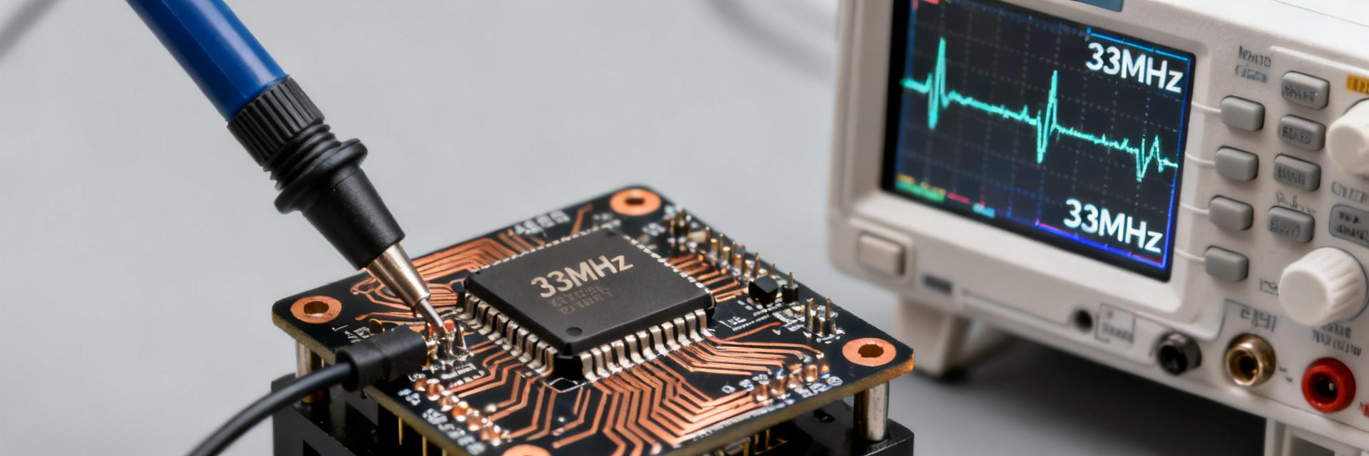
The DSA6041HA3B-038K000VAO is a 38 kHz CMOS oscillator that operates from 1.71–3.63 V, positioning it for ultra-low-voltage embedded designs and energy-constrained IoT nodes. This article delivers a full datasheet breakdown, precise pinout guidance, integration best practices, and a procurement checklist to accelerate PCB validation and production readiness.
Readers will find a compact spec snapshot, electrical and environmental analysis, recommended PCB footprint practices, measurement and debugging steps, and a procurement action list tailored for US engineering teams focused on low-power timing solutions.
1 — Product overview & key specs (background)
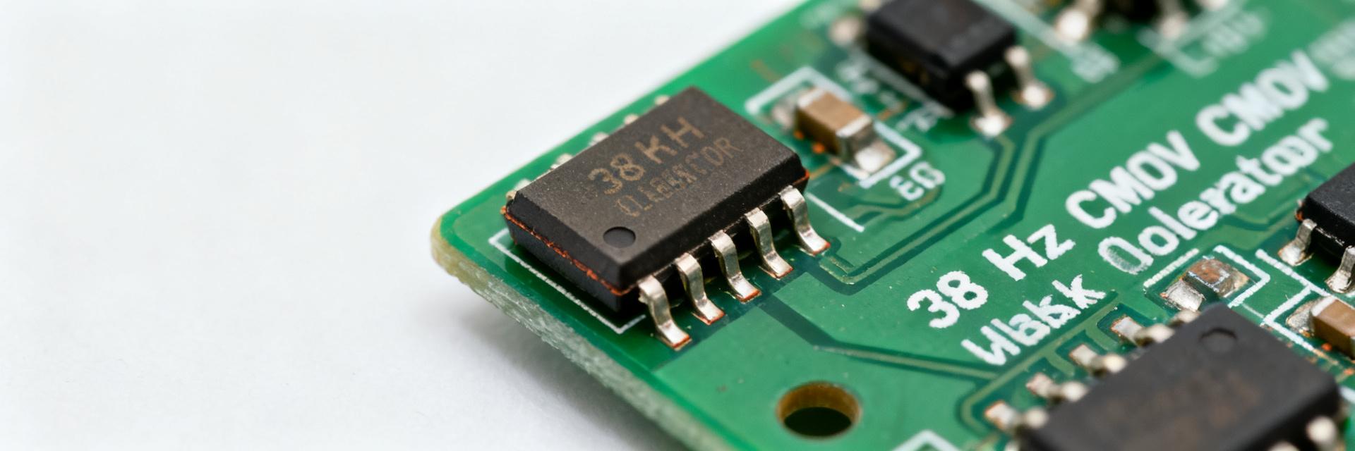
Quick spec snapshot
| Parameter | Specification Details |
|---|---|
| Nominal frequency | 38 kHz |
| Supply voltage range | 1.71–3.63 V |
| Package type | 4‑VFLGA |
| Enable/disable | Dedicated EN/disable input |
| Typical output type | CMOS push‑pull |
| Temperature grades | Consumer and industrial (typical industrial: −40°C to +85°C) |
At a glance: consult the official datasheet for absolute maximum ratings; expect low‑microamp standby currents and single‑digit mA active drive depending on load.
Typical applications & target audience
Common uses include real‑time wake timers, remote control infra‑red carriers, low‑frequency timing for sensor wake cycles, and small wearable or IoT nodes where board area and power are constrained. The part suits engineers optimizing for fixed low frequency, minimal BOM, and small footprint integration.
2 — Datasheet deep-dive: electrical & environmental specs (data analysis)
Electrical characteristics to extract and explain
Focus on VDD range, typical and maximum supply currents, CMOS output voltage swing, output drive (source/sink capability), EN input thresholds, startup time, and frequency stability (ppm over temperature). Include datasheet-derived tables for typical vs. max currents, a frequency vs. voltage curve, and an enable timing diagram when documenting behavior for system-level timing budgets.
Environmental, reliability & qualification notes
Key environmental items include operating temperature grade, ESD sensitivity class, moisture sensitivity level (MSL), and recommended reflow profile. For industrial use, prioritize parts with specified extended temperature bounds and higher ESD/MSL ratings; derate near thermal or vibration extremes and follow datasheet test conditions when defining qualification tests.
3 — Pinout & package details (method guide)
Pin-by-pin functions and signal descriptions
A typical 4‑pin oscillator pinout lists: Pin 1 VCC (power in), Pin 2 GND, Pin 3 OUT (CMOS output, push‑pull), Pin 4 EN (active high/low disable per datasheet). Recommended EN handling is a defined pull (10 kΩ typical) to set default state and an input filter or small series resistor to prevent glitches on power sequencing; refer to the pinout for valid voltage thresholds and direction.
PCB footprint, mechanical & thermal considerations
For the 4‑VFLGA footprint use the manufacturer‑recommended land pattern with solder mask defined pads and thermal vias if a central pad exists. Place a 0.1 µF decoupling capacitor within 1–2 mm of VCC pin, pour a solid ground plane under the device, and avoid routing noisy high‑current traces adjacent to the OUT node to minimize jitter and EMI coupling.
4 — Integration, testing & troubleshooting (method & practical)
Integration best practices
Power sequencing: ensure VCC rises smoothly with EN held in a defined state to avoid false oscillation. Decoupling: 0.1 µF ceramic in parallel with 1 µF bulk near VCC. Output routing: short, controlled‑impedance traces with a single series resistor (33–100 Ω) at the scope probe or line end to prevent reflections. Example reference circuit: VCC → decoupling caps → device VCC; EN → 10 kΩ pull to preferred state; OUT → series resistor → system input.
Measurement & debugging tips
Use a 10× scope probe with 50 Ω termination if measuring absolute amplitude; set scope bandwidth >100 kHz and enable averaging for jitter inspection. Typical waveforms are square CMOS levels; common failures include no output (check VCC/EN and decoupling), sub‑frequency shifts (check load, supply droop), and intermittent output (ESD or soldering defects). Follow a stepwise checklist: verify supply, confirm EN logic level, probe at package pad, then inspect solder joints and thermal conditions.
5 — Variants, procurement notes & practical checklist (case study + action)
Ordering codes, variant decoding & cross-reference advice
Ordering codes commonly append suffixes for frequency, temperature grade, and packaging (e.g., tape‑and‑reel vs. tray). Decode suffixes to confirm required frequency, industrial temperature grade, and packaging. For low‑power designs prioritize variants with lower standby current; for harsh environments choose industrial grade and confirm ESD/MSL classifications on the procurement spec.
BOM, compliance & on-board handling checklist
Procurement checklist: confirm full part number and revision, request the official datasheet and recommended land pattern, verify moisture sensitivity level and required dry storage, document ESD handling procedures, and plan alternative sources for lead‑time mitigation. Confirm RoHS/REACH status and add long‑tail procurement descriptors (e.g., "38 kHz CMOS oscillator 4‑VFLGA low voltage datasheet") to supplier queries.
Summary
The DSA6041HA3B-038K000VAO is a compact 38 kHz CMOS oscillator optimized for low‑voltage designs; engineers should validate supply range, output type, pinout, and thermal limits before layout. Download the official datasheet to confirm absolute ratings and follow the integration checklist for reliable deployment.
- Validate VDD and EN behavior against the datasheet; ensure decoupling and defined EN pull to avoid startup glitches and preserve timing integrity.
- Adopt the recommended 4‑VFLGA land pattern, place a 0.1 µF decoupling cap within 1–2 mm of VCC, and use a ground pour to reduce jitter and EMI.
- Use a controlled measurement setup (10× probe, appropriate termination) and follow a stepwise debug checklist: supply → EN → pad probe → solder and thermal inspection.
FAQ
What is the expected startup behavior for the oscillator when VDD is applied?
On VDD application, the part typically requires EN to be in the enabled state or released from a defined pull to begin oscillation; startup time is specified in the datasheet under test conditions. If oscillation does not start, verify VCC voltage, EN logic level, and decoupling proximity.
How should the EN pin be handled to prevent unintended toggles?
Tie EN to a defined logic level with a pull resistor (10 kΩ typical) and add a small series resistor or RC filter if the board’s power sequencing can create transients. Glitch protection prevents spurious toggles that can disrupt system timing.
What measurement settings are recommended to verify the 38 kHz output?
Use a 10× oscilloscope probe, >100 kHz scope bandwidth, and 50 Ω termination where amplitude accuracy is critical. Observe frequency stability over expected VCC and temperature ranges and compare results to datasheet tolerance specifications for pass/fail criteria.
Can the DSA6041HA3B-038K000VAO drive capacitive loads directly without a buffer?
It is highly recommended to minimize direct capacitive loading on the CMOS push-pull output. For loads exceeding 15 pF, integrate a series termination resistor (33–100 Ω) or an external buffer to prevent signal distortion, rise-time degradation, and excessive active current draw.